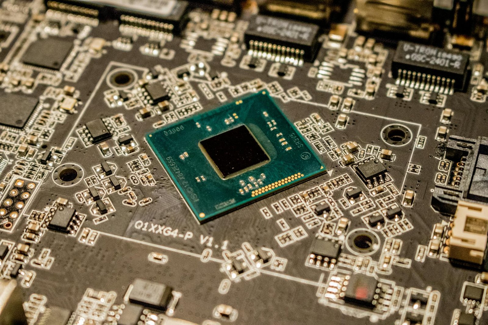
Wafer processing is a crucial aspect of Very Large-Scale Integration (VLSI) technology, which forms the foundation for modern semiconductor devices such as microprocessors, memory chips, and integrated circuits (ICs). This process involves a series of intricate steps aimed at transforming a silicon wafer into functional semiconductor devices capable of performing complex electronic functions. Here’s a comprehensive exploration of wafer processing in VLSI.
1. Wafer Preparation:
- Starting Material: High-purity silicon ingots are sliced into thin, circular wafers using precise cutting techniques. These wafers typically range from 150mm to 300mm in diameter and serve as the substrate for semiconductor fabrication.
- Cleaning: Wafers undergo rigorous cleaning processes to remove any impurities, particles, or contaminants that could affect the performance and reliability of the semiconductor devices.
2. Thin Film Deposition:
- Purpose: Thin films of various materials are deposited onto the wafer’s surface to create essential layers that form the basis of semiconductor components.
- Techniques: Chemical vapor deposition (CVD), physical vapor deposition (PVD), and atomic layer deposition (ALD) are commonly used to deposit materials like silicon dioxide (SiO₂), silicon nitride (Si₃N₄), metals (e.g., aluminum, copper), and polysilicon onto specific areas of the wafer.
3. Photolithography:
- Pattern Definition: Photolithography is a key process that defines the intricate patterns and structures of semiconductor components on the wafer.
- Steps Involved:
- Photoresist Coating: A layer of photoresist material is applied uniformly onto the wafer’s surface.
- Exposure: The wafer is exposed to ultraviolet (UV) light through a photomask, which contains the desired circuit pattern.
- Development: Chemicals are used to selectively remove the exposed (positive photoresist) or unexposed (negative photoresist) areas of the photoresist, revealing the underlying wafer material.
4. Etching:
- Pattern Transfer: Etching processes are employed to transfer the defined patterns from the photoresist layer onto the underlying wafer materials.
- Types of Etching: Wet etching uses liquid chemicals to remove materials, while dry etching (plasma etching) uses reactive gases and plasma to achieve higher precision and control.
5. Doping:
- Introduction of Dopants: Dopant atoms (e.g., phosphorus, boron) are selectively introduced into specific regions of the silicon wafer to modify its electrical properties.
- Ion Implantation: High-energy ions are accelerated and implanted into the wafer, penetrating its surface to create desired doping profiles.
6. Oxidation and Annealing:
- Oxidation: Thermal oxidation processes are used to grow silicon dioxide (SiO₂) layers on the wafer’s surface, serving as electrical insulators and protective barriers.
- Annealing: Heat treatments (thermal annealing) are applied to activate dopants, repair crystal damage caused by ion implantation, and optimize the electrical characteristics of the semiconductor devices.
7. Metallization and Interconnection:
- Metal Layer Deposition: Thin layers of metals (e.g., aluminum, copper) are deposited onto the wafer’s surface to create electrical contacts and interconnects between different semiconductor components.
- Patterning: Photolithography and etching processes define the precise locations and shapes of metal interconnects, ensuring reliable electrical connections and signal propagation across the semiconductor device.
8. Dielectric Deposition and Passivation:
- Dielectric Layers: Insulating materials such as silicon nitride (Si₃N₄) and silicon dioxide (SiO₂) are deposited to isolate and protect semiconductor components from electrical interference.
- Passivation: Surface passivation techniques enhance device reliability by forming protective layers that prevent moisture ingress, chemical contamination, and mechanical stress.
9. Testing and Quality Control:
- Electrical Testing: Each wafer undergoes comprehensive testing to evaluate its electrical characteristics, functionality, and performance under simulated operating conditions.
- Defect Inspection: Advanced inspection tools and techniques, including scanning electron microscopy (SEM) and optical inspection systems, detect and analyze defects that could impact semiconductor device reliability and yield.
10. Packaging and Assembly:
- Wafer Dicing: Wafers are diced into individual semiconductor devices (chips) containing the fabricated circuits and components.
- Packaging: Each chip is mounted onto a package substrate and connected to external leads or pins through wire bonding or flip-chip bonding techniques.
- Encapsulation: Chips are encapsulated in protective materials (e.g., epoxy resin) to safeguard against environmental factors, mechanical stress, and physical damage.
11. Final Testing and Yield Optimization:
- Functional Testing: Packaged semiconductor devices undergo final electrical testing to verify their functionality, performance, and reliability according to industry standards.
- Yield Enhancement: Statistical process control (SPC) methodologies and yield optimization strategies are employed to maximize the number of defect-free semiconductor devices per wafer, ensuring high manufacturing yield and cost-effectiveness.
12. Integration and Application:
- Device Integration: Finished semiconductor devices are integrated into electronic systems during device manufacturing, enabling their use in diverse applications such as computers, smartphones, automotive electronics, and industrial machinery.
- Lifecycle Management: Continuous monitoring, refinement, and improvement processes ensure ongoing quality, performance, and reliability of semiconductor devices throughout their operational lifecycle.
Advanced Technologies and Future Directions:
- Advanced Materials: Exploration of new semiconductor materials (e.g., gallium nitride, silicon carbide) with superior electrical properties for enhanced device performance and efficiency.
- Nanotechnology: Advancements in nanoscale fabrication techniques facilitate the production of smaller, more energy-efficient semiconductor devices with increased functionality and integration density.
In conclusion, wafer processing in VLSI technology represents a complex and meticulously controlled series of steps aimed at fabricating high-performance semiconductor devices. The integration of innovative materials, advanced manufacturing techniques, and rigorous quality assurance measures continues to drive the evolution of semiconductor technology, enabling the development of increasingly powerful and versatile electronic devices.


